STM of synthetic 2D devices
Stacking thin layer flakes like graphene, h-BN and transition metal dichalcogenides (TMDs) provides novel avenues to assemble synthetic compounds with electronic properties by design. Their great potential for novel functionalities inspire an intensive research effort worldwide.
Investigating the properties of these artificial materials by scanning tunneling microscopy and spectroscopy is very challenging due to the stringent constraints on their surface condition. Surface degradation and/or absorbates usually introduced during the stacking process and electron beam lithography (EBL), are often very difficult to be removed. We have learned to circumvent these limitation either by preventing or removing the absorbates using shadow mask evaporation and AFM cleaning. An attractive alternative is to protect the surface of interest by a thin capping layer.
Graphene in proximity to TMDs
The spin-orbit interaction (SOI) in graphene can be strongly enhanced by its proximity to a TMD. However, the strength of the SOI varies by an order of magnitude accross measurements from different research groups. Using quasiparticle interference (QPI) measurement, we find clear evidence for intravalley scattering on the graphene/TMD heterostructure. Such scattering is absent in bare graphene because it is forbidden by the chirality of the electron on graphene. The allowed backscattering provides valuable insight into the mass gap and SOI in the heterostructures (collaboration with Alberto Morpurgo and Louk Rademaker).
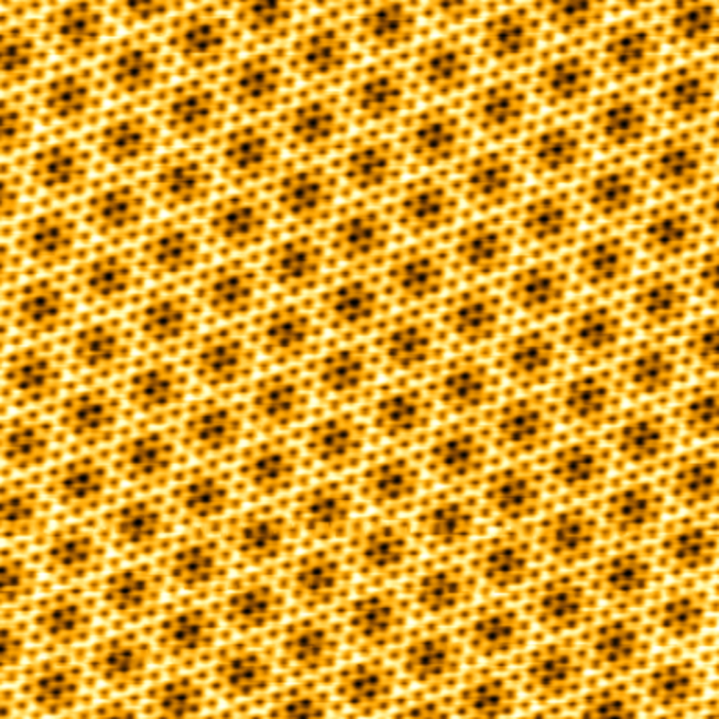
STM of NbSe2 through a MoS2 capping layer
In this study, we demonstrate that charge ordering can be imaged and the superconducting gap measured in 2H-NbSe2 by STM imaging and spectroscopy through a capping mono layer of MoS2 (Collaboration with Alberto Morpurgo).
