Dimensional crossover of the charge density wave transition in thin exfoliated VSe2
Published on September 4, 2017
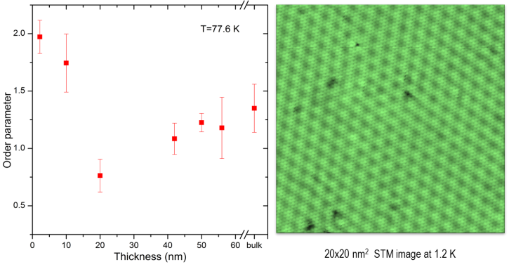
Scanning tunneling microscopy of in-situ exfoliated VSe2 reveals a non monotonic thickness dependence of the charge density wave (CDW) order parameter and phase transition temperature. Both parameters are extracted directly form the charge modulation amplitude imaged in STM micrographs. This study lifts the contradictions of previous experiments claiming opposite thickness dependencies of the CDW and shows thickness to be a true but non trivial tuning parameter of the electronic properties in layered materials.
Authors
Árpád Pásztor, Alessandro Scarfato, Céline Barreteau, Enrico Giannini and Christoph Renner
Published in
2D Materials 4, 041005 (2017)
See this publication on UNIGE